Scheme of a New Year's garland on a microcontroller. Features of repairing a Chinese LED garland Light machine on a microcontroller for a garland
The New Year is coming soon! Christmas tree decorations appear on store shelves next to tangerines, sweets and champagne: multi-colored balls, tinsel, all kinds of flags, beads and, of course, electric garlands.
You probably won’t be able to buy a regular garland of multi-colored light bulbs. But there are simply countless different flashing lights, mostly made in China. Microscopic bulbs can be placed on a piece of cardboard or woven into a carpet of wires that can be used to decorate an entire window at once.
Christmas tree garlands are also distinguished by great variety, especially in appearance and design. The cost of such garlands is low, as is the power of the light bulbs.
Most garlands have a small plastic box with one button, a cord with a power plug and wires going to a garland of multi-colored light bulbs. The design of the garland can be very diverse.
The simplest and cheapest option consists of microscopic light bulbs inserted. On the back of the packaging box there are instructions for replacing the bulbs and safety precautions, although no spare bulbs are included. These are the garlands that are sold in the “Everything for 38” chain of stores, although recently they have sold for forty rubles.

Figure 1. Garland for forty rubles
Garlands of another style have small plastic shades on the light bulbs, for example, in the form of transparent flowers with petals. But the box with the button remains the same, although the price of the garland reaches up to two hundred rubles. Let's try to open the box and see what's inside.
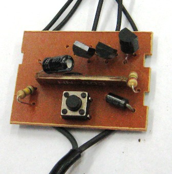
Figure 2. Appearance of a garland controller with three thyristors
At the bottom of the figure two wires are shown; this is how the device is connected to the network. There is also a button here that switches operating modes. In the upper part you can see three thyristors and wires going to the garlands.
In the middle of the board there is a black drop mounted on a small printed circuit board. The board has contact pads with which the controller is soldered into the main board.
How many thyristors are on the board
The control electrodes of thyristors, which turn on strings of light bulbs, are connected to the outputs of the microcontroller. The microcontroller has four outputs, but often, instead of four thyristors, only three are installed on the board, and in some cases only two.
The necessary visual effect is achieved by connecting garlands and placing light bulbs: light bulbs of two or even three colors are sealed in one garland. Just such a board is shown in Figure 2.
If you look at this board from the printed circuit board, you can see that three thyristors are soldered, and under the fourth there are holes with tinned contact pads, as shown in Figure 3. In some cases, the holes are not even drilled, they say, whoever wants to drill it himself .

Figure 3. Garland controller board. Free space for thyristor
Here it is worth noting this feature: if the controller output is not connected anywhere, this does not mean that it is not working. The program in all controllers is apparently the same, all controller outputs are used.
This can be easily verified using a pointer tester. If you measure the constant tension on the free leg, the needle will jump, twitch and deviate along with the blinking of other garlands. It is enough to simply solder the missing thyristor into the board, and, please, we get a full-fledged four-channel garland.
The thyristor can be taken from an old faulty board (it happens that the controller becomes unusable) or you can buy an additional garland for forty rubles and remove the thyristor from there. For a good cause, the costs are extremely small!
Schematic diagram of the garland
It is not difficult to draw a circuit diagram using a printed circuit board. There are two types of schemes, slightly different from each other. The first, most advanced option is shown in Figure 4.

Figure 4. Chinese garland controller. Option 1
The entire circuit is powered via VD1…VD4. The garlands are powered by pulsating voltage and are turned on by the controller through thyristors VS1...VS4. Resistor R1 and microcontroller DD1 form a voltage divider, the output of which is a voltage of 12V.
Capacitor C1 smoothes out the ripples of the rectified voltage. Through resistor R7, the mains voltage is supplied to the input of controller 1 to synchronize the circuit with the 220V mains frequency, which allows for phase control of the thyristors. This synchronization allows for smooth ignition and extinction of the garlands. These are the types of boards that can be found in expensive garlands.
The board shown in Figure 3 is assembled according to a somewhat simplified circuit, which is shown in Figure 5.

Figure 5. Chinese garland controller. Option 2
It immediately catches your eye that there are only three thyristors, and only one diode remains from the rectifier bridge. Resistors also disappeared from the control electrodes of the thyristors. But, in general, the consumer properties remained the same as in the previous circuit, despite the fact that the light bulbs light up only when there is a positive half-cycle of the mains voltage on the upper wire of the circuit. Without a rectifier bridge, half-wave rectification is obtained.
This version of the circuit design is inherent in those garlands that are “all forty”. That, in fact, is all that can be said about the circuit design of Chinese Christmas tree garlands.
How to connect powerful lamps
The power of the garlands is low, the bulbs are simply microscopic, and they are unlikely to fit anywhere else besides a home Christmas tree. But sometimes it is necessary to connect a garland with powerful incandescent lamps, for example, for decorative lighting of building facades. This modification has already been given in the article. The diagram of the modified garland is shown in Figure 8 in the mentioned article.
If you don't want to remake the board
It is much easier to do without reworking the controller board. All you have to do is make four powerful output switches with optocoupler isolations and connect them instead of low-power garlands. The power switch circuit is shown in Figure 6.

Figure 6. Powerful power switch with optocoupler isolation
Actually, the scheme is typical, it works flawlessly, and does not contain any pitfalls. As soon as the LED of the MOC3021 optocoupler lights up, the low-power optocoupler thyristor opens and the control electrode and the anode of the BTA16-600 triac are connected through pins 4, 6 and resistor R1. The triac opens and turns on the load, in this case a garland.
An optocoupler should be used without a built-in CrossZero circuit (line voltage zero crossing detector), for example, MOC3020, MOC3021, MOC3022, MOC3023. If the optocoupler has a CrossZero node, then the circuit WILL NOT WORK! This should not be forgotten.
The BTA16-600 triac has the following parameters: forward current 16A, reverse voltage 600V. At a current of 5A and a voltage of 220V, the load power is already a whole kilowatt. True, you will need to install a triac on the radiator.
The metal substrate is isolated from the crystal, as indicated by the letter A in the triac marking. This makes it possible to install triacs on a radiator without mica spacers and insulators for the screw. By the way, it is these triacs that are used in the power regulators of household vacuum cleaners, while the radiator is blown by the air flow at the outlet of the vacuum cleaner.
If the load power is no more than 400W, then you can do without a radiator. The pinout of the triac is shown in Figure 7.

Figure 7. Pinout of triac BTA16-600
This drawing will come in handy when assembling a power switch circuit. It is best to assemble all four power switches on a common printed circuit board. It is better to assemble resistor R from two 2W resistors, which will avoid their excessive heating. The maximum current of the input LED of the optocoupler is 50mA, so a current of 20...30mA will ensure its long-term trouble-free operation.

Figure 8. Connecting power switches to the controller board
In general, everything is clear and simple. The garlands are unsoldered from the controller, and the input circuits of the power switches are soldered in their place. In this case, no intervention is required in the printed circuit wiring of the controller. The only exception is the soldering of an additional thyristor, provided that it can be found. You will also have to make the power cord and plug somewhat thicker, since the original one has a very small cross-section.
If installed correctly and the parts are in good working order, the circuit does not need to be configured. The design of the device is arbitrary, preferably in a metal case of suitable dimensions, which will act as a radiator for triacs.
To ensure electrical safety, the device should be turned on via a circuit breaker, or at least a fuse.
There are many ways to decorate a Christmas tree, here is one of them.
Figure 1 shows a diagram of a New Year's garland. It contains four channels to which series-connected LEDs are connected, shown in Figure 2.

The core of the circuit is the PIC16F628A microcontroller. The microcontroller operates according to the algorithm shown in Figure 3. The program code is written in assembly language, see listing Garland\16F628ATEMP.ASM.

The full cycle of in-circuit programming and debugging of the PIC16F628A microcontroller was carried out using (integrated development environment), the MPASM v5.22 compiler (included in MPLAB IDE v8.15) and MPLAB ICD 2 (in-circuit debugger - “Debugger”). For those who do not have the tools listed above, but have their own program for working with HEX files and another programmer, you can find the file 16F628ATEMP.HEX in the corresponding project. The technical specification of the microcontroller can be found on the website and.
Microcontroller DD1 has functional outputs RB4 – RB7, to which amplifying MOSFET field-effect transistors VT1 – VT4 are connected. Technical specifications for transistors can be found on the website. The drains of the transistors are connected to push-in terminals X2 – X5. The load supply voltage is set by the circuit power supply, which is connected to connector X1. The maximum switched current per channel is 0.5 A. Microcontroller DD1 does not have a forced reset function; the reset pin is connected through resistor R1 to the positive supply potential. To generate the clock frequency, the microcontroller uses an on-chip clock generator. The device can be operated in the temperature range from – 40 °C to +85 °C.
The device is powered from an alternating or direct voltage source connected to connector X1. The rated voltage of the power supply is 12 V. The rated current of the power supply depends on the load and is 0.5 - 2 A. To stabilize the power supply, a conventional circuit is used: a diode bridge VD1, a linear stabilizer DA1, filter capacitors C1 - C4.
The microcontroller is programmed with 3 lighting effects, based on the “running lights” effect.
1) The garlands alternately light up and go out in one direction and repeat in the same way in the other direction.
2) The garlands light up one by one and when all four garlands are lit, they begin to go out one by one in the same direction, and the same is repeated in the reverse order.
3) 1 and 2, 3 and 4 garlands alternately wink at each other. The microcontroller is programmed to perform a predetermined number of repetitions of the lighting effect. It is worth noting that the time interval between the lighting of the garlands changes (increases, reaches a peak, and then falls), that is, the effect of “temporary swing” is visible. To better demonstrate the lighting effects, the garlands (as they are numbered in the diagram) should be placed in order in the same plane. In this case, decorate the spruce from the roots to the top (vertically, dividing the spruce into four sectors for garlands), from 1 to 4 garlands, respectively.
The power supply of the garlands is connected to the power source connected to connector X1, therefore it is necessary to calculate the series-connected light-emitting elements (LEDs, incandescent lamps). The total supply voltage is found from the sum of the voltages of the light-emitting elements connected in series. For example, there will be 6 series-connected bright LEDs designed for a voltage of 2 - 2.5 V in one garland. Since LEDs consume 20 mA, it is possible to connect series-connected LEDs in parallel in rows.
Installation of parts is one-sided. Hole sizes range from 0.7 mm to 3 mm. Files for making a printed circuit board can be found in the folder.

The printed circuit board is shown in Figure 4. The location of parts is shown in Figure 5.

The following parts can be replaced in this unit. Microcontroller DD1 from the PIC16F628A-I/P-xxx series with an operating clock frequency of 20 MHz in a DIP18 package. Voltage stabilizer DA1 domestic KR142EN5A (5 V, 1.5 A). MOSFET field-effect transistors and VT1 - VT4 (N-channel) in an I-Pak (TO-251AA) package, analogues of the ratings indicated in the diagram are suitable. Diode bridge VD1 for an operating voltage of at least 25 V and a current of at least 2 A. Power connector X1 is similar to that indicated in the diagram with a central contact d = 2.1 mm. Non-polar capacitors C1 and C2 with a nominal value of 0.01 – 0.47 µF x 50 V. Electrolytic capacitors C3 and C4 have the same capacitive rating, and the voltage is not lower than that indicated in the diagram. Multi-colored LEDs VD1 – VD6 for voltage 2 - 2.5 V.

List of radioelements
| Designation | Type | Denomination | Quantity | Note | Shop | My notepad |
|---|---|---|---|---|---|---|
| DD1 | MK PIC 8-bit | PIC16F628A | 1 | To notepad | ||
| DA1 | Linear regulator | L7805AB | 1 | KR142EN5A | To notepad | |
| VT1-VT4 | MOSFET transistor | IRLU024N | 4 | To notepad | ||
| VD1 | Diode bridge | 2W10M | 1 | To notepad | ||
| C1 | Capacitor | 0.1 µF | 1 | To notepad | ||
| C2 | Capacitor | 0.1 µF | 1 | To notepad | ||
| C3 | 100uF 10V | 1 | To notepad | |||
| C4 | Electrolytic capacitor | 220uF 25V | 1 |
As people say - prepare your sleigh in the summer...
You probably decorate the Christmas tree with all sorts of garlands for the New Year, and most likely they have long since become boring with the monotony of their blinking. I would like to do something so that, wow, it blinks just like on the capital’s Christmas trees, only on a smaller scale. Or, as a last resort, hang it on the window so that this beauty illuminates the city from the 5th floor.
But alas, there are no such garlands for sale.
Actually, this is exactly the problem that had to be solved two years ago. Moreover, due to laziness, 2 years passed from idea to implementation, as usual, and everything was done in the last month. Actually, you will have more time (or I don’t understand anything about human psychology, and everything will be done exactly the same in the last 2 weeks before the new year?).
The result is a fairly simple design of individual modules with LEDs, and one common one that transmits commands from the computer to the network of these modules.
The first version of the module was conceived to connect them to the network via two wires, so that there would be less confusion and all that - but it didn’t work out, in the end a fairly powerful and high-speed switch was required to switch the power of even a small number of modules - an obvious overkill for simplicity of design, so I gave preference the third wire is not so convenient, but it is much easier to organize a data transmission channel.
How everything works.

The developed network is capable of addressing up to 254 slave modules, which will be further called SLAVE - they are connected by only 3 wires, as you guessed - two wires are +12V power supply, common and the third is signal.
they have a simple scheme: 
As you can see, it supports 4 channels - Red, Green, Blue and Violet.
True, according to the results of practical testing, purple is clearly visible only close up, but how! Also, due to the fact that the colors are located too far from each other, the color mixing can only be seen from 10 meters away, if you use RGB LEDs the situation will be somewhat better.
In order to simplify the design, we also had to abandon quartz stabilization - firstly, the extra output is taken away and secondly, the cost of a quartz resonator is quite noticeable and thirdly, there is no urgent need for it.
A protective cascade is assembled on the transistor so that the controller port is not knocked out by static - the line can still be quite long, in extreme cases only the transistor will suffer. The cascade is calculated in MicroCap and has an approximate response threshold of about 7 volts and a weak dependence of the threshold on temperature.
Naturally, in the best traditions, all modules respond to address number 255 - this way you can turn them all off at the same time with one command.
A module called MASTER is also connected to the network - it is an intermediary between the PC and the network of slave SLAVE modules. Among other things, it is a source of reference time for synchronizing slave modules in the absence of quartz stabilization in them.
Scheme: 
The circuit contains optional potentiometers - they can be used in a program on a PC for convenient and quick adjustment of the desired parameters; at the moment this is implemented only in the test program in the form of the ability to assign any of the potentiometers to any of the 4 channels. The circuit is connected to a PC via a USB-UART interface converter on an FT232 chip.
An example of a packet sent to the network: 
Its beginning: 
Electrical characteristics of the signal: log.0 corresponds to +9...12V, and log.1 corresponds to 0...5V.
As you can see, data is transmitted sequentially, at a fixed speed of 4 bits. This is due to the necessary margin for error in the data reception speed - SLAVE modules do not have quartz stabilization, and this approach guarantees data reception with a deviation in the transmission speed of up to +-5% in excess of those that are compensated by the software method based on measuring the calibrated interval at the beginning of data transmission which provides resistance to reference frequency drift by another +-10%.
Actually, the algorithm of operation of the MASTER module is not so interesting (it is quite simple - we receive data via UART and forward it to the network of slave devices), all the most interesting solutions are implemented in SLAVE modules, which actually allow you to adapt to the transmission speed.
The main and most important algorithm is the implementation of a 4-channel 8-bit software PWM which allows you to control 4 LEDs with 256 gradations of brightness for each of them. The implementation of this algorithm in hardware also determines the data transfer rate on the network - for software convenience, one bit is transmitted for each step of PWM operation. A preliminary implementation of the algorithm showed that it runs in 44 clock cycles, so it was decided to use a timer configured to interrupt every 100 clock cycles - this way, the interrupt has time to be guaranteed to be executed before the next one and execute part of the code of the main program.
At the selected clock frequency of the internal oscillator of 4.8 MHz, interrupts occur at a frequency of 48 kHz - this is the bit speed the network of slave devices has and the PWM is filled at the same speed - as a result, the frequency of the PWM signal is 187.5 Hz, which is quite enough not to notice the flickering of the LEDs. Also, in the interrupt handler, after executing the algorithm responsible for generating PWM, the state of the data bus is recorded - it turns out approximately in the middle of the timer overflow interval, this simplifies data reception. At the beginning of receiving the next 4-bit packet, the timer is reset, this is necessary for more accurate reception synchronization and resistance to reception speed deviations.
The result is the following picture: 
The implementation of the algorithm for adjusting the transmission speed is interesting. At the beginning of the transmission, MASTER issues a pulse with a duration of 4 bits of log.0, from which all slave modules determine the required reception speed using a simple algorithm:
LDI tmp2, st_syn_delay DEC tmp2 ;<+ BREQ bad_sync ; | SBIC PINB, cmd_port; | RJMP PC-0x0003 ;-+
St_syn_delay = 60 - a constant that determines the maximum duration of the starting pulse, which is taken to be approximately 2 times the nominal value (for reliability)
Using an experimental method, the following dependence of the resulting number in tmp2 was established when the clock frequency deviates from the nominal:
4.3Mhz (-10%) 51 units (0x33) corresponds to 90 timer clocks to return the reception speed to nominal
4.8Mhz (+00%) 43 units (0x2B) - corresponds to 100 timer clocks (nominal)
5.3Mhz (+10%) 35 units (0x23) - corresponds to 110 timer clocks to return the reception speed to nominal
Based on these data, the correction factors for the timer interrupt period were calculated (this is how the reception speed is adjusted to the existing clock frequency of the controller):
Y(x) = 110-x*20/16
x = tmp2 - 35 = (0, 1, 2, 3, 4, 5, 6, 7, 8, 9, 10, 11, 12, 13, 14, 15, 16)
Y(x) = (110, 108.75, 107.5, 106.25, 105, 103.75, 102.5, 101.25, 100, 98.75, 97.5, 96.25, 95, 93.75, 92.5, 91.25, 90)
The numbers are rounded to whole numbers and stored in the EEPROM.
If, when applying voltage to the module, hold the line in the logical state “1”, a calibration subroutine will be activated, which will allow you to measure the period of the PWM signal with a frequency meter or oscilloscope without correction and, based on the measurements, judge the deviation of the clock frequency of the module controller from the nominal one, with a strong deviation of more than 15% The built-in RC oscillator calibration constant may need to be adjusted. Although the manufacturer promises calibration at the factory and deviation from the nominal value of no more than 10%.
At the moment, a Delphi program has been developed that allows you to reproduce a previously compiled pattern for 8 modules at a given speed. As well as a utility for working with a separate module (including reassigning the module address).
Firmware.
for the SLAVE module, only fuses CKSEL1 = 0 and SUT0 = 0 need to be flashed. The rest should be left unflashed. The contents of the EEPROM are flashed from the file RGBU-slave.eep, if necessary, you can immediately set the desired address of the module on the network - the 0th byte of the EEPROM, by default it is flashed as $FE = 254, address 0x13 contains the calibration constant of the built-in RC oscillator of the controller, at a frequency of 4.8 MHz it does not load automatically, so it is necessary to read the factory calibration value with the programmer and write it in this cell - this value is individual for each controller, with large frequency deviations from the nominal value, you can change the calibration through this cell without affecting the factory value.
For the MASTER module, it is necessary to flash only fuses SUT0 = 0, BOOTSZ0 = 0, BOOTSZ1 = 0, CKOPT = 0. Leave the rest unflashed.
Finally, a small demonstration of the garland located on the balcony:
In fact, the functionality of the garland is determined by the program on the PC - you can create color music, stylish iridescent room lighting (if you add LED drivers and use powerful LEDs) - etc. What do I plan to do in the future? The plans include a grid of 12 modules with 3-watt RGB LEDs, and room lighting based on pieces of 12-volt RGB tape (you only need field-effect transistors for switching the tape for each module, 3 pieces or 4 if you add a piece of purple tape other differences from there will be no original).
To manage the network, you can write your own program, even in BASIC - the main thing that the chosen programming language should do is be able to connect to immortal COM ports and configure their parameters. Instead of the USB interface, you can use an adapter with RS232 - this gives the potential ability to control lighting effects from a wide range of devices that can generally be programmed.
The exchange protocol with the MASTER device is quite simple - we send a command and wait for a response about its success or failure; if there is no response for more than a few milliseconds, there are problems with the connection or operation of the MASTER device, in which case it is necessary to carry out a reconnection procedure.
The following commands are currently available:
0x54; symbol “T” - command “test” - check the connection, the answer should be 0x2B.
0x40; the "@" symbol is the "download and transfer" command. After issuing the command, you need to wait for the response "?" followed by 6 bytes of data:
+0: Slave address 0..255
+1: Command to device
0x21 - bytes 2...5 contain channel brightness that must be applied immediately.
0x14 - set a timeout, after which the brightness on all channels will be
reset to 0 if no commands are received during this time. The timeout value is in the red channel cell, i.e. in a byte at offset +2. value 0-255 corresponds to a timeout of 0-25.5 seconds by default, timeout = 5 seconds (written in EEPROM during firmware, it can also be changed there in a byte with offset +1).
0x5A - change device address.
For reliability, the procedure for changing the address must be performed three times - only then will the new address be applied and registered in the EEPROM. At the same time, you need to be careful - if you assign the same address to two devices, they will react synchronously, and you can “separate” them only by physically disconnecting the extra modules from the network and changing the address of the remaining one, or using a programmer. The value of the new address is transmitted in the red channel cell - i.e. in a byte at offset +2.
2: Red brightness 0...255
+3: Green brightness 0...255
+4: Blue brightness 0...255
+5: Violet brightness 0...255
0x3D; symbol "=" - ADC command. After issuing the command, you need to wait for the response "?" then 1 byte should be transmitted - the ADC channel number 0..7 in binary form (ASCII numbers 0..9 are also suitable in this capacity, since the highest 4 bits are ignored).
In response, the command returns 2 bytes of the measurement result in the range 0...1023
Possible responses to commands:
0x3F; symbol "?" - ready for data input, means that the device is ready to receive command arguments
0x2B; symbol "+" Response - command executed
0x2D; symbol "-" Response - the command is not defined or is incorrect
More details can be obtained from the source code located on GitHub, where the latest versions of ready-made firmware are also located.
Happy New Year, dear users. And for the upcoming holiday, the electronic portal site decided to please you with a New Year's garland circuit on a PIC microcontroller. Let's move on to reviewing this device.
It contains four channels to which series-connected LEDs are connected, shown in the figure below:

The core of the circuit is the PIC16F628A microcontroller. The program code is written in assembly language, see listing Garland16F628ATEMP.ASM. The full cycle of in-circuit programming and debugging of the PIC16F628A microcontroller was carried out using MPLAB IDE v8.15 (integrated development environment), the MPASM v5.22 compiler (included in MPLAB IDE v8.15) and MPLAB ICD 2 (in-circuit debugger - “Debugger”). For those who do not have the tools listed above, but have their own program for working with HEX files and another programmer, you can find the file 16F628ATEMP.HEX in the corresponding project.
Microcontroller DD1 has functional outputs RB4 - RB7, to which amplifying MOSFET field-effect transistors VT1 - VT4 are connected. Technical specifications for transistors can be found on the website. The transistor drains are connected to push-in terminals X2 - X5. The load supply voltage is set by the circuit power supply, which is connected to connector X1. The maximum switched current per channel is 0.5 A. Microcontroller DD1 does not have a forced reset function; the reset pin is connected through resistor R1 to the positive supply potential. To generate the clock frequency, the microcontroller uses an on-chip clock generator. The device can be operated in the temperature range from - 40 °C to +85 °C.
The device is powered from an alternating or direct voltage source connected to connector X1. The rated voltage of the power supply is 12 V. The rated current of the power supply depends on the load and is 0.5 - 2 A. To stabilize the power supply, a conventional circuit is used: a diode bridge VD1, a linear stabilizer DA1, and filter capacitors C1 - C4.
The microcontroller is programmed with 3 lighting effects, based on the “running lights” effect:
- The garlands alternately light up and go out in one direction and repeat in the same way in the other direction.
- The garlands light up one by one and when all four garlands are lit, they begin to go out one by one in the same direction, and the same is repeated in the reverse order.
- Garlands 1 and 2, 3 and 4 alternately wink at each other.
The microcontroller is programmed to perform a predetermined number of repetitions of the lighting effect. It is worth noting that the time interval between the lighting of the garlands changes (increases, reaches a peak, and then falls), that is, the effect of “temporary swing” is visible. To better demonstrate the lighting effects, the garlands (as they are numbered in the diagram) should be placed in order in the same plane. In this case, decorate the spruce from the roots to the top (vertically, dividing the spruce into four sectors for garlands), from 1 to 4 garlands, respectively.
The power supply of the garlands is connected to the power source connected to connector X1, therefore it is necessary to calculate the series-connected light-emitting elements (LEDs, incandescent lamps). The total supply voltage is found from the sum of the voltages of the light-emitting elements connected in series. For example, there will be 6 series-connected bright LEDs designed for a voltage of 2 - 2.5 V in one garland. Since LEDs consume 20 mA, it is possible to connect series-connected LEDs in parallel in rows.


The following parts can be replaced in this unit. Microcontroller DD1 from the PIC16F628A-I/P-xxx series with an operating clock frequency of 20 MHz in a DIP18 package. Voltage stabilizer DA1 domestic KR142EN5A (5 V, 1.5 A). MOSFET field-effect transistors and VT1 - VT4 (N-channel) in an I-Pak (TO-251AA) package, analogues of the ratings indicated in the diagram are suitable. Diode bridge VD1 for an operating voltage of at least 25 V and a current of at least 2 A. Power connector X1 is similar to that indicated in the diagram with a central contact d = 2.1 mm. Non-polar capacitors C1 and C2 with a nominal value of 0.01 - 0.47 µF x 50 V. Electrolytic capacitors C3 and C4 have the same capacitive rating, and the voltage is not lower than that indicated in the diagram. Multi-colored LEDs VD1 - VD6 for voltage 2 - 2.5 V.
| This diagram is also often viewed: |
We have already learned earlier, but it is much more interesting to control this process using buttons, and the LED garland will serve as a good visual example.
Connecting a button to a microcontroller
The garland diagram is shown below.

When a button (key) is connected to a microcontroller, the corresponding MK pin must be configured as an input. In this case, the microcontroller will constantly read the state, or rather the potential level at this pin. Therefore, the program algorithm can be constructed in such a way that if at a certain pin of the MK the potential changes from high to low or vice versa, then a certain action will be performed, for example, an LED will light up.
To configure certain pins of the MK as input, zeros should be written to the corresponding bits of the DDR register. By the way, if the MK pins are not used, then it is also recommended to configure them for input. Since we will only connect buttons to port B, we will write all zeros to the DDRB register with the following command:
DDRB = 0b00000000;
When a microcontroller pin is configured as an input, it can initially be in two states, which are set using the PORT register.

If the PORT register bit is set to zero, then the pin has a high input impedance.
When the bit is set to one, a pull-up resistor is connected to the MK pin. The resistor is so called because through it a high potential (+ 5 V) is “pulled up” to the corresponding point in the electrical circuit; in this case - to the pin of the microcontroller.
Checking the status of the MK output using PINx
To know at any time what potential is present at the pin, you should check (read) the corresponding bit in the PIN register.
By analogy, this register can be compared with a sensor. You can only read information from it. You can't write anything to it. PIN is the opposite of the PORT register, which only writes to, but does not read, data.
It is more preferable to set the PORT register to one, i.e. use of internal pull-up resistor MK. This option has significant noise immunity, since to change the high potential to a low one, the output must be directly connected to ground or a common wire.
If the pin is made with a high input resistance, then any more or less powerful electromagnetic interference can induce a certain potential on it that exceeds a certain value and the microcontroller will perceive the interference as a change from low potential to high. Therefore, in our program we will use an internal pull-up resistor.
We connect one contact of the key to ground (common wire), and the second to the pin of the microcontroller. When the key is open, the output is at a high potential (+ 5 V), pulled up by the internal resistor of the MK. In this case, the corresponding bit of the PIN register will be set to one.
When you press the button, this pin will connect to the common wire (“minus”) and a low potential will appear on it. And the PIN register bit will automatically be set to zero.
Please note that the pull-up resistor also protects the circuit from a short circuit when the button is pressed.
LED garland in code
Now let's write the entire program code, and then look at its individual elements. The algorithm of the program is as follows: when the first key is closed, the “lights” will turn on in one sequence, and when the second is closed, the “lights” will light up differently. If both buttons are pressed, then all LEDs should be off.
#define F_CPU 1000000UL // Declare the operating frequency of the microcontroller 1 MHz
#include
#include
#define Z 300 // Name the delay value Z
#define VD PORTD // Assign the name VD to port D
#define K PORTB // Assign the name K to port B, to which the buttons are connected
int main(void)
DDRB = 0b00000000; // Configure port B for input
DDRD = 0b11111111; // Configure port D for output
VD = 0b00000000; // Turn off all lights
K = 0b11111111; // Turn on pull-up resistors
while (1)
if (PINB == 0b11111110) // Check if the 1st button is pressed
VD = 0b11111111; // If the key is closed, then we flash the “lights”
_delay_ms(Z);
VD = 0b00000000;
_delay_ms(Z);
else
VD = 0b00000000; // If the key is open, then all LEDs are turned off
if (PINB == 0b11111101) // Check if the 2nd button is pressed
VD = 0b00000001; // If the button is pressed, then turn on the LED one by one
_ delay_ ms(Z); // with a delay of 0.3 s
VD = 0b00000011;
_delay_ms(Z);
VD = 0b00000111;
_delay_ms(Z);
VD = 0b00001111;
_delay_ms(Z);
LED = 0b00011111;
_delay_ms(Z);
VD = 0b00111111;
_delay_ms(Z);
VD = 0b01111111;
_ delay_ms(Z);
VD = 0b11111111;
_delay_ms(Z);
VD = 0b00000000;
_ delay_ ms(Z);
else
VD = 0b00000000; // If the key is not closed, then all LEDs are turned off
Operators if And else
The purpose of preprocessors and them are well known from previous articles. What's new to us here is the if statement. If is translated from English as “if”. If the condition specified in parentheses is met, i.e. true, then the program code inside the curly braces is executed. For example, if variable a is greater than 1 unit, then variable c will be assigned the value a + b.
if (a >1)
c = a + b;
Otherwise, when the value of a is less than or equal to one, the program code in the curly braces will not be executed.
If only one command is executed in curly braces, then the C syntax allows you to simplify the notation and do without curly braces:
if (a >1) c = a + b;
The if statement also works in conjunction with the else statement.
if (a >1) → if a >1, then = a + b
c = a + b;
else → otherwise, c = a - b
c = a - b;
It works like this. If a > 1, then c = a + b. Otherwise, i.e. when a is less than or equal to one, then c = a – b.
Explanation of the program code
Now let's return to our program. If the button connected to PB0 is pressed, then a low potential appears on the pin and the corresponding bit of the PINB register is set to zero. In this case, the condition in curly brackets will be fulfilled, i.e. the garland will start flashing.
Note that the assignment command consists of one equal sign "=", and the command to test the condition "equals" consists of two equal signs written without a space "==".
When the button is not pressed, the PINB register bit will show a one caused by the pull-up resistor being high. In this case, control will pass to the else statement and all LEDs will be turned off.
When the second key is closed, the output of which is connected to port PB1, the second program code will be executed, and the LEDs will begin to turn on one by one with a time delay of 0.3 seconds.
Thus, a garland on a microcontroller can contain a different number of LEDs and keys. Moreover, for each closing or opening of the key contacts, you can prescribe your own algorithm for the operation of the garland.
It can also be controlled with just one button. This option has a slightly more complicated code, and we will consider it in a separate article. There we will also look at how to connect powerful LEDs to the MK.

Earlier in the article, you looked in detail at setting up the output, and here - for the input. Now let's put everything together and present a simple visual algorithm.


